Resources tagged nanometer-process-nodes
-
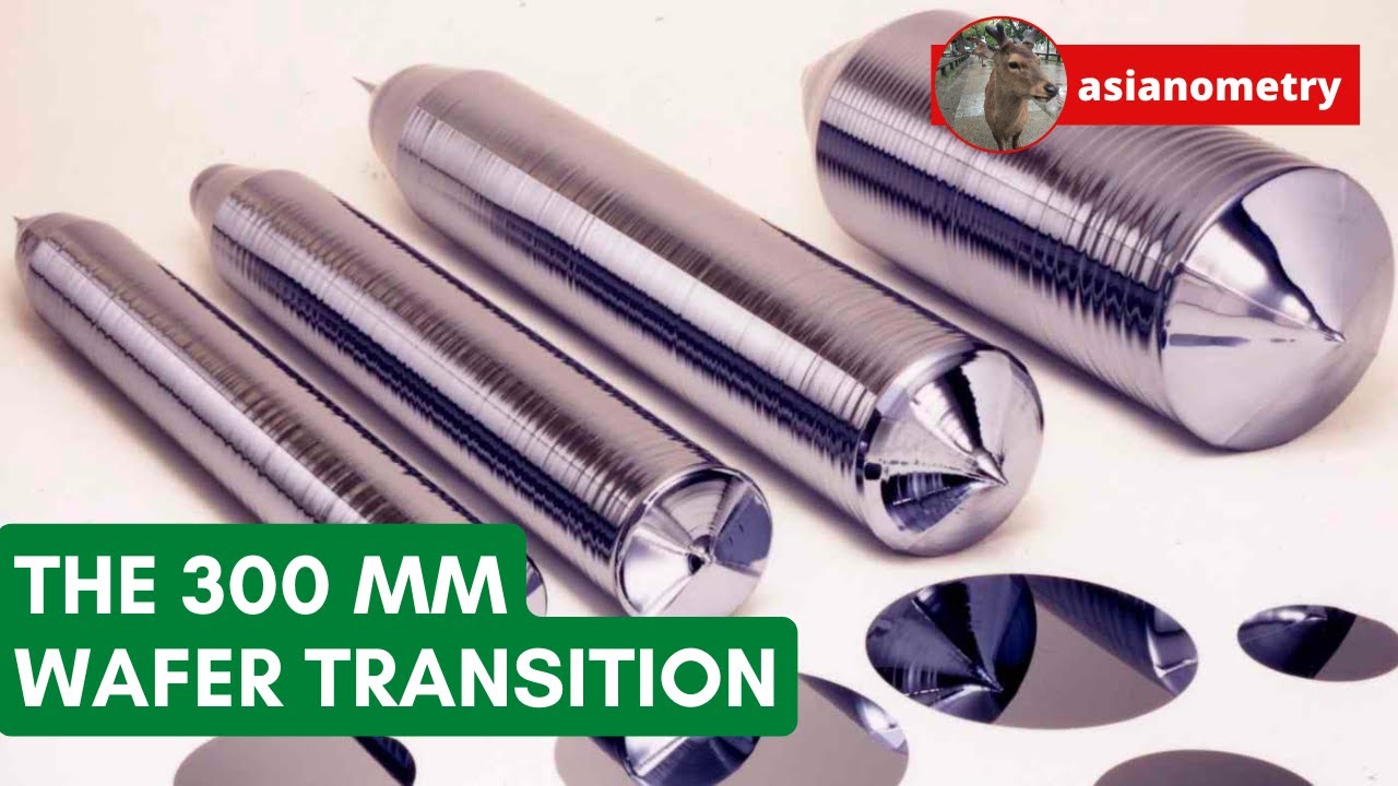
Asianometry - The 300mm Silicon Wafer Transition, 05082022
At the turn of the century, the $200 billion semiconductor manufacturing industry across the globe joined hands and underwent a massive transition ... This video looks at the semiconductor industry's momentous transition from using 200 millimeter silicon wafers to 300 millimeter wafers in their manufacturing process It also outlines how a pure silicon wafer crystal made (i.e. grown, cut, polished and delivered); the productivity rate; and potential defects during this process
Get full access to our construction knowledge base, latest news and updates ... Join the discussion.